Electronics and Communication Engineering - Electronic Devices and Circuits
Exercise : Electronic Devices and Circuits - Section 1
- Electronic Devices and Circuits - Section 1
- Electronic Devices and Circuits - Section 2
- Electronic Devices and Circuits - Section 3
- Electronic Devices and Circuits - Section 4
- Electronic Devices and Circuits - Section 5
- Electronic Devices and Circuits - Section 6
- Electronic Devices and Circuits - Section 7
- Electronic Devices and Circuits - Section 8
- Electronic Devices and Circuits - Section 9
- Electronic Devices and Circuits - Section 10
- Electronic Devices and Circuits - Section 11
- Electronic Devices and Circuits - Section 12
- Electronic Devices and Circuits - Section 13
- Electronic Devices and Circuits - Section 14
- Electronic Devices and Circuits - Section 15
- Electronic Devices and Circuits - Section 16
1.
At room temperature the current in an intrinsic semiconductor is due to
Answer: Option
Explanation:
Intrinsic material has equal number of holes and electrons.
2.
Work function is the maximum energy required by the fastest electron at 0 K to escape from the metal surface.
Answer: Option
Explanation:
Work function is the minimum energy required by the fastest electron at 0 K to escape from the metal surface.
3.
The most commonly used semiconductor material is
Answer: Option
Explanation:
Germanium is rarely used.
4.
In which of these is reverse recovery time nearly zero?
Answer: Option
Explanation:
In schottky diode there is no charge storage and hence almost zero reverse recovery time.
5.
A transistor has a current gain of 0.99 in the CB mode. Its current gain in the CC mode is
Answer: Option
Explanation:
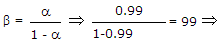 Current gain = 1 + β = 100.
Quick links
Quantitative Aptitude
Verbal (English)
Reasoning
Programming
Interview
Placement Papers