Electronics and Communication Engineering - Electronic Devices and Circuits
Exercise : Electronic Devices and Circuits - Section 8
- Electronic Devices and Circuits - Section 1
- Electronic Devices and Circuits - Section 2
- Electronic Devices and Circuits - Section 3
- Electronic Devices and Circuits - Section 4
- Electronic Devices and Circuits - Section 5
- Electronic Devices and Circuits - Section 6
- Electronic Devices and Circuits - Section 7
- Electronic Devices and Circuits - Section 8
- Electronic Devices and Circuits - Section 9
- Electronic Devices and Circuits - Section 10
- Electronic Devices and Circuits - Section 11
- Electronic Devices and Circuits - Section 12
- Electronic Devices and Circuits - Section 13
- Electronic Devices and Circuits - Section 14
- Electronic Devices and Circuits - Section 15
- Electronic Devices and Circuits - Section 16
1.
Assertion (A): Hall effect is used to find the type of semiconductor.
Reason (R): When a specimen of semiconductor carrying current I lies in a magnetic field the force on electrons and holes is in opposite directions.
2.
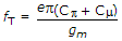
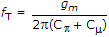
The fT of a BJT is related to its gm, Cp and Cμ as follows.


3.
When a p-n junction is forward biased. The width of depletion layer decreases.
4.
In which of the following case the rating of the transformer to deliver 100 watts of d.c. power to a load, will be least?
5.
When a p-n Junction is forward biased
Quick links
Quantitative Aptitude
Verbal (English)
Reasoning
Programming
Interview
Placement Papers