Electronics and Communication Engineering - Electronic Devices and Circuits
Exercise : Electronic Devices and Circuits - Section 1
- Electronic Devices and Circuits - Section 1
- Electronic Devices and Circuits - Section 2
- Electronic Devices and Circuits - Section 3
- Electronic Devices and Circuits - Section 4
- Electronic Devices and Circuits - Section 5
- Electronic Devices and Circuits - Section 6
- Electronic Devices and Circuits - Section 7
- Electronic Devices and Circuits - Section 8
- Electronic Devices and Circuits - Section 9
- Electronic Devices and Circuits - Section 10
- Electronic Devices and Circuits - Section 11
- Electronic Devices and Circuits - Section 12
- Electronic Devices and Circuits - Section 13
- Electronic Devices and Circuits - Section 14
- Electronic Devices and Circuits - Section 15
- Electronic Devices and Circuits - Section 16
6.
In p-n-p transistor the current IE has two components viz. IEP due to injection of holes from p-region to n-region and IE due to injection of electrons from n-region to p-region. Then
Answer: Option
Explanation:
Emitter is p-type in p-n-p transistor.
Therefore holes are majority carriers.
7.
In an n channel JFET, the gate is
Answer: Option
Explanation:
Since channel is n type gate must be p type.
8.
The amount of photoelectric emission current depends on
Answer: Option
Explanation:
Only the intensity of incident radiation governs the amount of photoelectric emission.
9.
Assertion (A): A p-n junction has high resistance in reverse direction.
Reason (R): When a reverse bias is applied to p-n junction, the width of depletion layer increases.
Answer: Option
Explanation:
The increase in reverse resistance is due to widening of depletion layer.
10.
In the circuit of figure the function of resistor R and diode D are
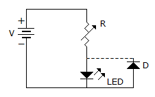
Answer: Option
Explanation:
Resistance limits current and diode is reverse connected and therefore protects LED against reverse breakdown.
Quick links
Quantitative Aptitude
Verbal (English)
Reasoning
Programming
Interview
Placement Papers