Electronics and Communication Engineering - Electronic Devices and Circuits
Exercise : Electronic Devices and Circuits - Section 2
- Electronic Devices and Circuits - Section 1
- Electronic Devices and Circuits - Section 2
- Electronic Devices and Circuits - Section 3
- Electronic Devices and Circuits - Section 4
- Electronic Devices and Circuits - Section 5
- Electronic Devices and Circuits - Section 6
- Electronic Devices and Circuits - Section 7
- Electronic Devices and Circuits - Section 8
- Electronic Devices and Circuits - Section 9
- Electronic Devices and Circuits - Section 10
- Electronic Devices and Circuits - Section 11
- Electronic Devices and Circuits - Section 12
- Electronic Devices and Circuits - Section 13
- Electronic Devices and Circuits - Section 14
- Electronic Devices and Circuits - Section 15
- Electronic Devices and Circuits - Section 16
31.
The static characteristic of an adequately forward biased P-n junction is a straight line, if the plot is of __________ Vs → versus
Answer: Option
Explanation:
Diode current equation
I = Is(eV/Vr - 1) 
 = eV/Vr - 1
=  = eVs/VR
 =
= 
Vs = VR .
32.
In an n channel JFET
Answer: Option
Explanation:
All currents are assumed positive when flowing into JFET.
33.
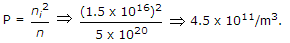
The intrinsic carrier concentration of silicon sample at 300 K is 1.5 x 10¹⁶/m3. If after doping, the number of majority carriers is 5 x 10²⁰/m3. The minority carrier density is
Answer: Option
Explanation:
34.
A diode is operating in forward region and the forward voltage and current are v = 3 + 0.3 sin ωt (volts) and i = 5 + 0.2 sin ωt (mA). The average power dissipated is
Answer: Option
Explanation:
The contribution of sine terms to power dissipation is zero.
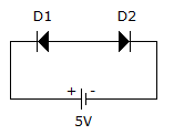
35.
Two identical silicon diodes D1 and D2 are connected back to back shown in figure. The reverse saturation current Is of each diode is 10-8 amps and the breakdown voltage VBr is 50 v. Evaluate the voltages VD1 and VD2 dropped across the diodes D1 and D2 assuming KT/q to be 25 m V.
Answer: Option
Explanation:
According to figure, D2 is forward bias, D1 is reverse biased. Reverse saturation current I0 = 10-8A. in clockwise direction.
For Diode D2 Is = I0
Here Is = I0
eqv2/kT = 2 or ev2/0.026 = 2
V2 = 0.018 V
Drop across D1 = V1 = 5 - 0.018
4.98 V
By KVL in mesh, VD1 = -4.98 V, VD2 = 0.018 V.
Quick links
Quantitative Aptitude
Verbal (English)
Reasoning
Programming
Interview
Placement Papers