Electronics and Communication Engineering - Electronic Devices and Circuits
Exercise : Electronic Devices and Circuits - Section 2
- Electronic Devices and Circuits - Section 1
- Electronic Devices and Circuits - Section 2
- Electronic Devices and Circuits - Section 3
- Electronic Devices and Circuits - Section 4
- Electronic Devices and Circuits - Section 5
- Electronic Devices and Circuits - Section 6
- Electronic Devices and Circuits - Section 7
- Electronic Devices and Circuits - Section 8
- Electronic Devices and Circuits - Section 9
- Electronic Devices and Circuits - Section 10
- Electronic Devices and Circuits - Section 11
- Electronic Devices and Circuits - Section 12
- Electronic Devices and Circuits - Section 13
- Electronic Devices and Circuits - Section 14
- Electronic Devices and Circuits - Section 15
- Electronic Devices and Circuits - Section 16
26.
The mean free path of conduction electrons in copper is about 4 x 10⁻⁸ m. For a copper block, find the electric field which can give, on an average, 1 eV energy to a conduction electron
Answer: Option
Explanation:
Work (Energy) = F x d
 1 eV = e.E x d
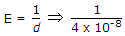
2.5 x 10⁷ V/m.
27.
When a p-n-p transistor is properly biased to operate in active region the holes from emitter.
Answer: Option
Explanation:
The reason that collector current is nearly equal to emitter current.
28.
Assertion (A): Silicon is preferred over germanium in manufacture of semiconductor devices.
Reason (R): Forbidden gap in silicon is more than that in germanium.
Answer: Option
Explanation:
Wider forbidden gap in silicon makes it less sensitive to temperature than germanium.
29.
Assertion (A): A decrease in temperature increases the reverse saturation current in a p-n diode.
Reason (R): When a diode is reverse biased surface leakage current flows.
Answer: Option
Explanation:
A is wrong because decrease in junction temperature decreases reverse saturation current.
30.
At room temperature a semiconductor material is
Answer: Option
Explanation:
At 0 K a semiconductor is perfect insulator. At room temperature it is slightly conducting.
Quick links
Quantitative Aptitude
Verbal (English)
Reasoning
Programming
Interview
Placement Papers