Electronics and Communication Engineering - Electronic Devices and Circuits
Exercise : Electronic Devices and Circuits - Section 14
- Electronic Devices and Circuits - Section 1
- Electronic Devices and Circuits - Section 2
- Electronic Devices and Circuits - Section 3
- Electronic Devices and Circuits - Section 4
- Electronic Devices and Circuits - Section 5
- Electronic Devices and Circuits - Section 6
- Electronic Devices and Circuits - Section 7
- Electronic Devices and Circuits - Section 8
- Electronic Devices and Circuits - Section 9
- Electronic Devices and Circuits - Section 10
- Electronic Devices and Circuits - Section 11
- Electronic Devices and Circuits - Section 12
- Electronic Devices and Circuits - Section 13
- Electronic Devices and Circuits - Section 14
- Electronic Devices and Circuits - Section 15
- Electronic Devices and Circuits - Section 16
26.
From an n channel JFET for VDS constant and if VGS is made more negative, pinch off would occur at
27.
The diode and the moving coil milliammeter of figure are assumed to be ideal. The meter reading is
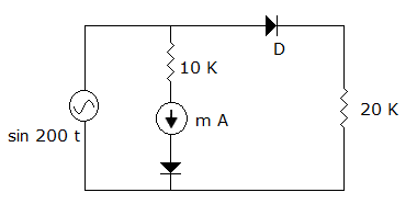
0.1 mA


28.
Measurement of Hall coefficient enables the determination of
29.
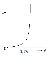
The V-I characteristic of a semi-conductor diode is shown in figure. From this figure it can be concluded that
30.
The process of deliberately adding impurity to a semi-conductor material is called
Quick links
Quantitative Aptitude
Verbal (English)
Reasoning
Programming
Interview
Placement Papers