Electronics and Communication Engineering - Electronic Devices and Circuits
Exercise : Electronic Devices and Circuits - Section 4
- Electronic Devices and Circuits - Section 1
- Electronic Devices and Circuits - Section 2
- Electronic Devices and Circuits - Section 3
- Electronic Devices and Circuits - Section 4
- Electronic Devices and Circuits - Section 5
- Electronic Devices and Circuits - Section 6
- Electronic Devices and Circuits - Section 7
- Electronic Devices and Circuits - Section 8
- Electronic Devices and Circuits - Section 9
- Electronic Devices and Circuits - Section 10
- Electronic Devices and Circuits - Section 11
- Electronic Devices and Circuits - Section 12
- Electronic Devices and Circuits - Section 13
- Electronic Devices and Circuits - Section 14
- Electronic Devices and Circuits - Section 15
- Electronic Devices and Circuits - Section 16
6.
A Si sample is doped with a fixed number of group N impurities. The electron density n is measured from 4 K to 1200 k for the sample. Which one of the following is correct?
7.
Assertion (A): In design of circuit using BJT, a derating factor is used.
Reason (R): As the ambient temperature increases, heat dissipation becomes slower.
Answer: Option
Explanation:
Increase of ambient temperature lowers the heat dissipation capacity.
Therefore derated operation of BJT is necessary lest BJT should be destroyed.
8.
If the drift velocity of holes under a field gradient of 100 V/m is 5m/sec. Their mobility is
Answer: Option
Explanation:
E = μ . Vd  μ =
μ = .
.
9.
In a P type silicon sample, the hole concentration is 2.25 x 10¹⁵ / cm3. If the intrinsic carrier concentration is 1.5 x 10¹⁰/ cm3 the electron concentration is
Answer: Option
Explanation:
Electron concentration 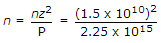 .
.
10.
The behaviour of a JFET is similar to that of
Answer: Option
Explanation:
Both JFET and vacuum triode are voltage controlled devices.
Quick links
Quantitative Aptitude
Verbal (English)
Reasoning
Programming
Interview
Placement Papers