Electronics and Communication Engineering - Electronic Devices and Circuits
Exercise : Electronic Devices and Circuits - Section 2
- Electronic Devices and Circuits - Section 1
- Electronic Devices and Circuits - Section 2
- Electronic Devices and Circuits - Section 3
- Electronic Devices and Circuits - Section 4
- Electronic Devices and Circuits - Section 5
- Electronic Devices and Circuits - Section 6
- Electronic Devices and Circuits - Section 7
- Electronic Devices and Circuits - Section 8
- Electronic Devices and Circuits - Section 9
- Electronic Devices and Circuits - Section 10
- Electronic Devices and Circuits - Section 11
- Electronic Devices and Circuits - Section 12
- Electronic Devices and Circuits - Section 13
- Electronic Devices and Circuits - Section 14
- Electronic Devices and Circuits - Section 15
- Electronic Devices and Circuits - Section 16
41.
The drain characteristics of JFET in operating region, are
Answer: Option
Explanation:
The drain current is almost constant. Therefore, characteristics is flat.
42.
As temperature increases
Answer: Option
Explanation:
Therefore, conductivity increases.
43.
When a reverse bias is applied to a p-n junction, the width of depletion layer.
Answer: Option
Explanation:
Therefore, the resistance is very high.
44.
The Hall constant in Si bar is given by 5 x 103 cm3/ coulomb, the hole concentration in the bar is given by
Answer: Option
Explanation:
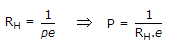 .
.
45.
Which of the following devices has a silicon dioxide layer?
Answer: Option
Explanation:
The SiO2 layer provides very high input impedance.
Quick links
Quantitative Aptitude
Verbal (English)
Reasoning
Programming
Interview
Placement Papers