Electronics and Communication Engineering - Electronic Devices and Circuits
Exercise : Electronic Devices and Circuits - Section 1
- Electronic Devices and Circuits - Section 1
- Electronic Devices and Circuits - Section 2
- Electronic Devices and Circuits - Section 3
- Electronic Devices and Circuits - Section 4
- Electronic Devices and Circuits - Section 5
- Electronic Devices and Circuits - Section 6
- Electronic Devices and Circuits - Section 7
- Electronic Devices and Circuits - Section 8
- Electronic Devices and Circuits - Section 9
- Electronic Devices and Circuits - Section 10
- Electronic Devices and Circuits - Section 11
- Electronic Devices and Circuits - Section 12
- Electronic Devices and Circuits - Section 13
- Electronic Devices and Circuits - Section 14
- Electronic Devices and Circuits - Section 15
- Electronic Devices and Circuits - Section 16
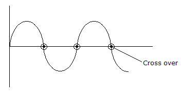
26.
Crossover distortion behaviour is characteristic of
Answer: Option
Explanation:
It is a characteristics of class B output stage as the amplifier is biased in cut-off region.
In class B amplifier, two transistor are operated in such a way that one is amplify the half cycle and second is amplify -ve half cycle.
27.
If aac for transistor is 0.98 then βac is equal to
Answer: Option
Explanation:
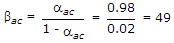 .
.
28.
Assertion (A): The conductivity of p type semiconductor is higher than that of intrinsic semiconductor.
Reason (R): The addition of donor impurity creates additional energy levels below conduction band.
Answer: Option
Explanation:
A refers to type semiconductor while R refers to n type semiconductor. Both A and R are correct but independent.
29.
In an n-p-n transistor biased for operation in forward active region
Answer: Option
Explanation:
In forward active mode emitter base junction is forward biased and base collector junction is reverse biased.
30.
An increase in temperature increases the width of depletion layer.
Answer: Option
Explanation:
With increase in temperature width of depletion layer decreases.
Quick links
Quantitative Aptitude
Verbal (English)
Reasoning
Programming
Interview
Placement Papers