Electronics and Communication Engineering - Electronic Devices and Circuits
Exercise : Electronic Devices and Circuits - Section 12
- Electronic Devices and Circuits - Section 1
- Electronic Devices and Circuits - Section 2
- Electronic Devices and Circuits - Section 3
- Electronic Devices and Circuits - Section 4
- Electronic Devices and Circuits - Section 5
- Electronic Devices and Circuits - Section 6
- Electronic Devices and Circuits - Section 7
- Electronic Devices and Circuits - Section 8
- Electronic Devices and Circuits - Section 9
- Electronic Devices and Circuits - Section 10
- Electronic Devices and Circuits - Section 11
- Electronic Devices and Circuits - Section 12
- Electronic Devices and Circuits - Section 13
- Electronic Devices and Circuits - Section 14
- Electronic Devices and Circuits - Section 15
- Electronic Devices and Circuits - Section 16
26.
The density of states (i.e. number of states per eV per m3) in the conduction band for energy level E is proportional to
27.
A-P type material has an acceptor ion concentration of 1 x 10¹⁶ per cm3. Its intrinsic carrier concentration is 1.48 x 10¹⁰/ cm. The hole and electron mobilities are 0.05m2/V-sec and 0.13 m2/V-sec respectively calculate the resistivity of the material
28.
Resistivity is a property of a semiconductor that depends on
29.
Operating point signifies that
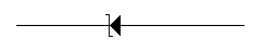
30.
Figure represents a
Quick links
Quantitative Aptitude
Verbal (English)
Reasoning
Programming
Interview
Placement Papers