Electronics and Communication Engineering - Electronic Devices and Circuits
Exercise : Electronic Devices and Circuits - Section 9
- Electronic Devices and Circuits - Section 1
- Electronic Devices and Circuits - Section 2
- Electronic Devices and Circuits - Section 3
- Electronic Devices and Circuits - Section 4
- Electronic Devices and Circuits - Section 5
- Electronic Devices and Circuits - Section 6
- Electronic Devices and Circuits - Section 7
- Electronic Devices and Circuits - Section 8
- Electronic Devices and Circuits - Section 9
- Electronic Devices and Circuits - Section 10
- Electronic Devices and Circuits - Section 11
- Electronic Devices and Circuits - Section 12
- Electronic Devices and Circuits - Section 13
- Electronic Devices and Circuits - Section 14
- Electronic Devices and Circuits - Section 15
- Electronic Devices and Circuits - Section 16
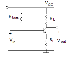
31.
In the BJT amplifier shown in the figure is the transistor is biased in the forward active region. Putting a capacitor across RE will
32.
In a centre tap full wave rectifier, 50 V is the peak voltage between the centre tap and one of the ends of the secondary. The maximum voltage across the reverse biased diode will be
33.
Consider the following statements.
The functions of an oxide layer in an IC device is to
The functions of an oxide layer in an IC device is to
- mask against diffusion or ion implant
- insulate the surface electrically
- increase the melting point of silicon
- produce a chemically stable protective layer of these statements.
34.
The forbidden energy gap for germanium is
35.
If the gate of JFET is reverse biased, the width of depletion region
Quick links
Quantitative Aptitude
Verbal (English)
Reasoning
Programming
Interview
Placement Papers