Electronics and Communication Engineering - Exam Questions Papers
Exercise : Exam Questions Papers - Exam Paper 12
- Exam Questions Papers - Exam Paper 12
- Exam Questions Papers - Exam Paper 22
- Exam Questions Papers - Exam Paper 21
- Exam Questions Papers - Exam Paper 20
- Exam Questions Papers - Exam Paper 19
- Exam Questions Papers - Exam Paper 18
- Exam Questions Papers - Exam Paper 17
- Exam Questions Papers - Exam Paper 16
- Exam Questions Papers - Exam Paper 15
- Exam Questions Papers - Exam Paper 14
- Exam Questions Papers - Exam Paper 13
- Exam Questions Papers - Exam Paper 1
- Exam Questions Papers - Exam Paper 11
- Exam Questions Papers - Exam Paper 10
- Exam Questions Papers - Exam Paper 9
- Exam Questions Papers - Exam Paper 8
- Exam Questions Papers - Exam Paper 7
- Exam Questions Papers - Exam Paper 6
- Exam Questions Papers - Exam Paper 5
- Exam Questions Papers - Exam Paper 4
- Exam Questions Papers - Exam Paper 3
- Exam Questions Papers - Exam Paper 2
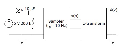
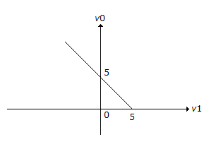
21.
In the following network, the switch is closed at t = 0 and the sampling starts from t = 0. The sampling frequency is 10Hz.
The samples x(n) (n = 0, 1, 2, ...) are given by
The samples x(n) (n = 0, 1, 2, ...) are given by
Answer: Option
Explanation:
Initial voltage across R = 5Vn
Final voltage across R = 0V
Thus VR = 5.0-0.5t
When we sample this at f∂ = 102
We get x(n) =  .
.
22.
Find 'X' in the circuit below:
f1(A, B, C, D) = Σ(6, 7, 13, 14);
f2(A, B, C, D) = Σ(3, 6, 7);
f3(A, B, C, D) = Σ(5, 6, 7, 14, 15)
f1(A, B, C, D) = Σ(6, 7, 13, 14);
f2(A, B, C, D) = Σ(3, 6, 7);
f3(A, B, C, D) = Σ(5, 6, 7, 14, 15)
Answer: Option
Explanation:
f1(A, B, C, D) = ∑(6, 7, 13, 14)
f2(A, B, C, D) = ∑(3, 6, 7)
f1 ⊕ f2 = ∑(3, 13, 14)
f3 x (f1 ⊕ f2) = ∑(14)= Y
X = f1 x Y = ∑(14).
23.
In the following circuit , the comparator output in log: "I" if V1 > V2 and is logic "0" otherwise. The D/A conversion is done as per the relations VDAC =  2n-2 Volts, where b3 (MSB), b2, b1 and b0 (LSB) are the counter outputs. The counter starts from the clear state
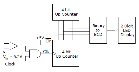
The stable reading of the LED display is
2n-2 Volts, where b3 (MSB), b2, b1 and b0 (LSB) are the counter outputs. The counter starts from the clear stateThe stable reading of the LED display is
Answer: Option
Explanation:
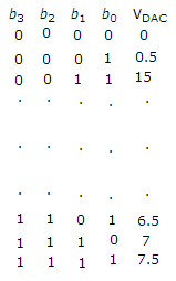
Using the given VDAC relation we can get tc
Thus stable reading of LED is 6.5 x 2 = 13.
24.
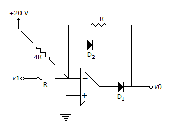
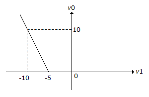
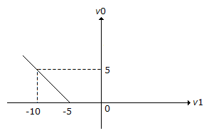
The transfer characteristic for the precision rectifier circuit shown below is (assume ideal OP-AMP and practical diodes)
Answer: Option
Explanation:
When Vi = - 10 V0 = 5.
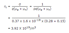
25.
If the intrinsic resistivity at 300°K is 0.37 ohm-m and the electron and hole mobilities at 300°K are 0.28 and 0.15 m2/volt-sec, then the intrinsic carrier concentration of Germanium is __________ .
Answer: Option
Explanation:
Quick links
Quantitative Aptitude
Verbal (English)
Reasoning
Programming
Interview
Placement Papers