Online Digital Electronics Test - Digital Electronics Test - Random
Instruction:
- This is a FREE online test. Beware of scammers who ask for money to attend this test.
- Total number of questions: 20.
- Time allotted: 30 minutes.
- Each question carries 1 mark; there are no negative marks.
- DO NOT refresh the page.
- All the best!
Marks : 2/20
Total number of questions
20
Number of answered questions
0
Number of unanswered questions
20
Test Review : View answers and explanation for this test.
1.
A DAC changes ________.
Your Answer: Option
(Not Answered)
Correct Answer: Option
Discuss about this problem : Discuss in Forum
Learn more problems on : Digital Concepts
2.
Give the decimal value of binary 10010.
Your Answer: Option
(Not Answered)
Correct Answer: Option
Discuss about this problem : Discuss in Forum
Learn more problems on : Digital Concepts
3.
Convert decimal 213 to binary.
Your Answer: Option
(Not Answered)
Correct Answer: Option
Discuss about this problem : Discuss in Forum
Learn more problems on : Number Systems and Codes
4.
The VHDL editor provided with a schematic editor development system will produce a file with the extension .vhd, which can be used by the simulator to test the output of the logic design.
Your Answer: Option
(Not Answered)
Correct Answer: Option
Discuss about this problem : Discuss in Forum
Learn more problems on : Boolean Algebra and Logic Simplification
5.
When is a flip-flop said to be transparent?
Your Answer: Option
(Not Answered)
Correct Answer: Option
Discuss about this problem : Discuss in Forum
Learn more problems on : Flip-Flops
6.
What is the significance of the J and K terminals on the J-K flip-flop?
Your Answer: Option
(Not Answered)
Correct Answer: Option
Discuss about this problem : Discuss in Forum
Learn more problems on : Flip-Flops
7.
A positive edge-triggered D flip-flop will store a 1 when ________.
Your Answer: Option
(Not Answered)
Correct Answer: Option
Discuss about this problem : Discuss in Forum
Learn more problems on : Flip-Flops
8.
For a multistage counter to be truly synchronous, the ________ of each stage must be connected to ________.
Cp, the same clock input line
CE, the same clock input line
 , the terminal count output
 , both clock input lines
Your Answer: Option
(Not Answered)
Correct Answer: Option
Discuss about this problem : Discuss in Forum
Learn more problems on : Counters
9.
Four cascaded modulus-10 counters have an overall modulus of ________.
Your Answer: Option
(Not Answered)
Correct Answer: Option
Discuss about this problem : Discuss in Forum
Learn more problems on : Counters
10.
When a computer is executing a program of instructions, the CPU will ________ memory locations as dictated by the program instructions.
Your Answer: Option
(Not Answered)
Correct Answer: Option
Discuss about this problem : Discuss in Forum
Learn more problems on : Memory and Storage
11.
What is occurring when two or more sources of data attempt to use the same bus?
Your Answer: Option
(Not Answered)
Correct Answer: Option
Discuss about this problem : Discuss in Forum
Learn more problems on : Computers
12.
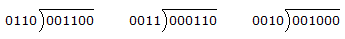
Divide the following binary numbers.
Your Answer: Option
(Not Answered)
Correct Answer: Option
Discuss about this problem : Discuss in Forum
Learn more problems on : Digital Arithmetic Operations and Circuits
13.
When the 2's-complement system is used, the number to be subtracted is changed to its 2's complement and then added to the minuend.
Your Answer: Option
(Not Answered)
Correct Answer: Option
Discuss about this problem : Discuss in Forum
Learn more problems on : Digital Arithmetic Operations and Circuits
14.
The AD7524, a CMOS IC available from several IC manufacturers, is an eight-bit D/A converter that uses a(n) ________.
sample-and-hold circuit
R/2R ladder network
multiplexer
10  s clock
s clockYour Answer: Option
(Not Answered)
Correct Answer: Option
Discuss about this problem : Discuss in Forum
Learn more problems on : Interfacing to the Analog World
15.
An indication of cutoff in an NPN bipolar transistor is that the:
Your Answer: Option
(Not Answered)
Correct Answer: Option
Discuss about this problem : Discuss in Forum
Learn more problems on : Signals and Switches
16.
Why is parallel data transmission preferred over serial data transmission for most applications?
Your Answer: Option
(Not Answered)
Correct Answer: Option
Discuss about this problem : Discuss in Forum
Learn more problems on : Signals and Switches
17.
Which type of gate can be used to add two bits?
Your Answer: Option
(Not Answered)
Correct Answer: Option
Discuss about this problem : Discuss in Forum
Learn more problems on : Ex-OR and Ex-NOR Gates
18.
The devices that provide the means for a computer to communicate with the user or other computers are referred to as:
Your Answer: Option
(Not Answered)
Correct Answer: Option
Discuss about this problem : Discuss in Forum
Learn more problems on : Microprocessor Fundamentals
19.
When the 8051 is reset and the EA line is LOW, the program counter points to the first program instruction in the:
Your Answer: Option
(Not Answered)
Correct Answer: Option
Discuss about this problem : Discuss in Forum
Learn more problems on : The 8051 Microcontroller
20.
The total external data memory that can be interfaced to the 8051 is:
Your Answer: Option
(Not Answered)
Correct Answer: Option
Discuss about this problem : Discuss in Forum
Learn more problems on : The 8051 Microcontroller
*** END OF THE TEST ***
Time Left: 00:29:56
Post your test result / feedback here:
Quick links
Quantitative Aptitude
Verbal (English)
Reasoning
Programming
Interview
Placement Papers