Digital Electronics - Memory and Storage
Why should I learn to solve Digital Electronics questions and answers section on "Memory and Storage"?
Learn and practise solving Digital Electronics questions and answers section on "Memory and Storage" to enhance your skills so that you can clear interviews, competitive examinations, and various entrance tests (CAT, GATE, GRE, MAT, bank exams, railway exams, etc.) with full confidence.
Where can I get the Digital Electronics questions and answers section on "Memory and Storage"?
IndiaBIX provides you with numerous Digital Electronics questions and answers based on "Memory and Storage" along with fully solved examples and detailed explanations that will be easy to understand.
Where can I get the Digital Electronics section on "Memory and Storage" MCQ-type interview questions and answers (objective type, multiple choice)?
Here you can find multiple-choice Digital Electronics questions and answers based on "Memory and Storage" for your placement interviews and competitive exams. Objective-type and true-or-false-type questions are given too.
How do I download the Digital Electronics questions and answers section on "Memory and Storage" in PDF format?
You can download the Digital Electronics quiz questions and answers section on "Memory and Storage" as PDF files or eBooks.
How do I solve Digital Electronics quiz problems based on "Memory and Storage"?
You can easily solve Digital Electronics quiz problems based on "Memory and Storage" by practising the given exercises, including shortcuts and tricks.
- Memory and Storage - General Questions
- Memory and Storage - True or False
- Memory and Storage - Filling the Blanks
Refer to the given figures (a) and (b). A logic analyzer is used to check the circuit in figure (a) and displays the waveforms shown in figure (b). The actual analyzer display shows all four data outputs, Q0-Q3. The analyzer's cursor is placed at position X and all four of the data output lines show a LOW level output. What is wrong, if anything, with the circuit?
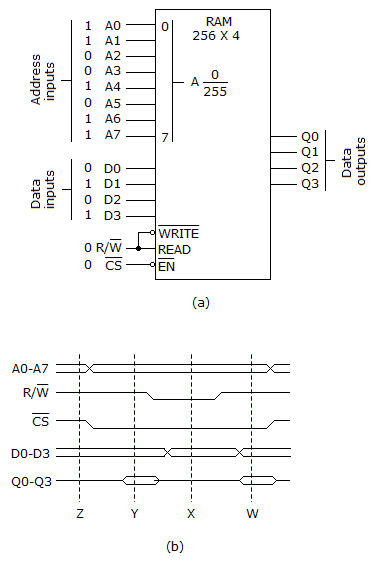
 mode and should be writing the contents of the selected address to Q0–Q3.