Electronics and Communication Engineering - Exam Questions Papers
Exercise : Exam Questions Papers - Exam Paper 15
- Exam Questions Papers - Exam Paper 12
- Exam Questions Papers - Exam Paper 22
- Exam Questions Papers - Exam Paper 21
- Exam Questions Papers - Exam Paper 20
- Exam Questions Papers - Exam Paper 19
- Exam Questions Papers - Exam Paper 18
- Exam Questions Papers - Exam Paper 17
- Exam Questions Papers - Exam Paper 16
- Exam Questions Papers - Exam Paper 15
- Exam Questions Papers - Exam Paper 14
- Exam Questions Papers - Exam Paper 13
- Exam Questions Papers - Exam Paper 1
- Exam Questions Papers - Exam Paper 11
- Exam Questions Papers - Exam Paper 10
- Exam Questions Papers - Exam Paper 9
- Exam Questions Papers - Exam Paper 8
- Exam Questions Papers - Exam Paper 7
- Exam Questions Papers - Exam Paper 6
- Exam Questions Papers - Exam Paper 5
- Exam Questions Papers - Exam Paper 4
- Exam Questions Papers - Exam Paper 3
- Exam Questions Papers - Exam Paper 2
41.
For a message signal m(t) = cos (2pfmt) and the carrier frequency fc, which of the following represents a single side band (SSB) signal?
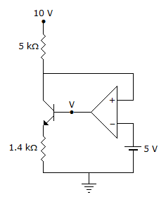
42.
In the circuit shown below, the op-amp is ideal, the transistor has VBE = 0.6 V and β = 150. Decide whether the feedback in the circuit is positive or negative and determine the voltage V at the output of the op-amp
43.
Which of the following addressing modes is used in the instruction PUSH B?
44.
Consider a silicon p-n junction at room temperature having the following parameters:
Doping on the n-side = 1 x 1017 cm-3
Depletion width on the n-side = 0.1 μm
Depletion width on the p-side = 1.0 μm
Intrinsic carrier concentration = 1.4 x 10¹⁴F. cm-1.
Thermal voltage = 26mV
Permittivity of free space = 8.85 x 10⁻¹⁴F. cm-1.
Dielectric constant of silicon = 12. The peak electric field in the device is
45.
A single turn loop is situated in air, with a uniform magnetic field normal to its plane. The area of the loop is 5 m2 and the rate of change of flux density is 2 Wb/m2/s. What is the emf appearing at the terminals of the loop?
Quick links
Quantitative Aptitude
Verbal (English)
Reasoning
Programming
Interview
Placement Papers