Electronics and Communication Engineering - Analog Electronics
Exercise : Analog Electronics - Section 3
- Analog Electronics - Section 11
- Analog Electronics - Section 21
- Analog Electronics - Section 20
- Analog Electronics - Section 19
- Analog Electronics - Section 18
- Analog Electronics - Section 17
- Analog Electronics - Section 16
- Analog Electronics - Section 15
- Analog Electronics - Section 14
- Analog Electronics - Section 13
- Analog Electronics - Section 12
- Analog Electronics - Section 1
- Analog Electronics - Section 10
- Analog Electronics - Section 9
- Analog Electronics - Section 8
- Analog Electronics - Section 7
- Analog Electronics - Section 6
- Analog Electronics - Section 5
- Analog Electronics - Section 4
- Analog Electronics - Section 3
- Analog Electronics - Section 2
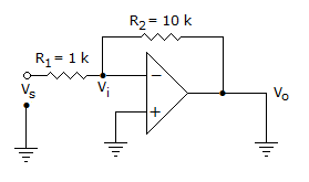
16.
The inverting op-amp shown in the figure has an open loop gain to 100. The closed loop given  is
is
isAnswer: Option
Explanation:
Applying KCL inverting node
 .
.
17.
In a voltage regulated power supply the zener operates in the breakdown region when (Vin is input voltage and Vz is zener breakdown voltage)
Answer: Option
Explanation:
Zener breakdown when input voltage is more than zener breakdown voltage.
18.
The parameter h11 for CB circuit is higher than that for CE circuit.
Answer: Option
Explanation:
It is lower.
19.
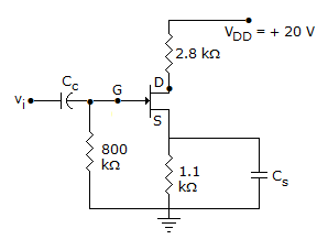
Figure shows a self bias circuit for FET amplifier, ID = 4 mA. Then IS =
Answer: Option
Explanation:
Since gate current is negligible IS = ID = 4 mA.
20.
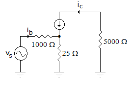
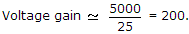
In the CE equivalent circuit of figure, the voltage gain is
Answer: Option
Explanation:
Quick links
Quantitative Aptitude
Verbal (English)
Reasoning
Programming
Interview
Placement Papers