Electronic Devices - DC Biasing-FETs
Exercise : DC Biasing-FETs - Filling the Blanks
- DC Biasing-FETs - General Questions
- DC Biasing-FETs - Filling the Blanks
11.
In a feedback-bias configuration, the slope of the dc load line is controlled by ________.
12.
For R2 smaller than ________ k the voltage VD is equal to VDD = 16 V.
the voltage VD is equal to VDD = 16 V. 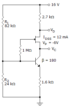
13.
In a depletion-type MOSFET, the transfer characteristic rises ________ as VGS becomes more positive.
14.
The dc load line is drawn using the equation obtained by applying Kirchhoff's voltage law (KVL) at ________ side loop(s) of the circuit.
15.
In a universal JFET bias curve, the vertical scale labeled m is used to find the solution to the ________ configuration.
Quick links
Quantitative Aptitude
Verbal (English)
Reasoning
Programming
Interview
Placement Papers