Online Electronic Devices Test - Electronic Devices Test 7
Instruction:
- This is a FREE online test. Beware of scammers who ask for money to attend this test.
- Total number of questions: 20.
- Time allotted: 30 minutes.
- Each question carries 1 mark; there are no negative marks.
- DO NOT refresh the page.
- All the best!
Marks : 2/20
Total number of questions
20
Number of answered questions
0
Number of unanswered questions
20
Test Review : View answers and explanation for this test.
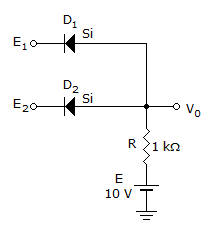
1.
What is the logic function of this circuit?
Your Answer: Option
(Not Answered)
Correct Answer: Option
Discuss about this problem : Discuss in Forum
Learn more problems on : Diode Applications
2.
What is the most frequently encountered transistor configuration?
Your Answer: Option
(Not Answered)
Correct Answer: Option
Discuss about this problem : Discuss in Forum
Learn more problems on : BJT Devices
3.
For practical transistors the level of alpha typically extends from ________ to ________ with most approaching the higher end of the range.
Your Answer: Option
(Not Answered)
Correct Answer: Option
Discuss about this problem : Discuss in Forum
Learn more problems on : BJT Devices
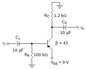
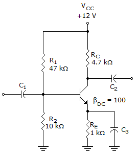
4.
Calculate VCE.
Your Answer: Option
(Not Answered)
Correct Answer: Option
Discuss about this problem : Discuss in Forum
Learn more problems on : DC Biasing-BJTs
5.
In an FET transistor, the depletion region is ________ near the top of both p-type materials.
Your Answer: Option
(Not Answered)
Correct Answer: Option
Discuss about this problem : Discuss in Forum
Learn more problems on : FET Devices
6.
The enhancement-type MOSFET is in the cutoff region if ________.
Your Answer: Option
(Not Answered)
Correct Answer: Option
Discuss about this problem : Discuss in Forum
Learn more problems on : FET Devices
7.
In the hybrid  or Giacoletto model, which one of the following does rb include?
or Giacoletto model, which one of the following does rb include?Your Answer: Option
(Not Answered)
Correct Answer: Option
Discuss about this problem : Discuss in Forum
Learn more problems on : BJT and FET Frequency Response
8.
For any inverting amplifier, the impedance capacitance will be ________ by a Miller effect capacitance sensitive to the gain of the amplifier and the interelectrode capacitance.
Your Answer: Option
(Not Answered)
Correct Answer: Option
Discuss about this problem : Discuss in Forum
Learn more problems on : BJT and FET Frequency Response
9.
If the parasitic capacitors were the only elements to determine the high cutoff frequency, the ________ frequency would be the determining factor.
Your Answer: Option
(Not Answered)
Correct Answer: Option
Discuss about this problem : Discuss in Forum
Learn more problems on : BJT and FET Frequency Response
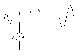
10.
This circuit is an example of a ________.
Your Answer: Option
(Not Answered)
Correct Answer: Option
Discuss about this problem : Discuss in Forum
Learn more problems on : Operational Amplifiers
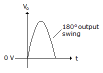
11.
This is an example of the output swing for a class ________ amplifier.
Your Answer: Option
(Not Answered)
Correct Answer: Option
Discuss about this problem : Discuss in Forum
Learn more problems on : Power Amplifiers
12.
Refer to this figure. The dc voltage on the collector, VC, is
Your Answer: Option
(Not Answered)
Correct Answer: Option
Discuss about this problem : Discuss in Forum
Learn more problems on : Power Amplifiers
13.
What is the first phase of the dual-slope method of conversion?
Your Answer: Option
(Not Answered)
Correct Answer: Option
Discuss about this problem : Discuss in Forum
Learn more problems on : Linear-Digital ICs
14.
The frequency distortion arising because of varying amplifier gain with frequency is considerably reduced in a negative-voltage feedback amplifier circuit.
Your Answer: Option
(Not Answered)
Correct Answer: Option
Discuss about this problem : Discuss in Forum
Learn more problems on : Oscillator Circuits
15.
This is an equivalent circuit for the ________ diode.

Your Answer: Option
(Not Answered)
Correct Answer: Option
Discuss about this problem : Discuss in Forum
Learn more problems on : Two-Terminal Devices
16.
Refer to this figure. Which symbol is correct for a zener diode?

Your Answer: Option
(Not Answered)
Correct Answer: Option
Discuss about this problem : Discuss in Forum
Learn more problems on : Special-Purpose Diodes
17.
In a class B push-pull amplifier, crossover distortion occurs when both transistors are off and the input signal voltage must exceed VBE before a transistor conducts.
Your Answer: Option
(Not Answered)
Correct Answer: Option
Discuss about this problem : Discuss in Forum
Learn more problems on : Power Amplifiers
18.
An E-MOSFET can be operated with either positive or negative values of VGS.
Your Answer: Option
(Not Answered)
Correct Answer: Option
Discuss about this problem : Discuss in Forum
Learn more problems on : Field-Effect Transistors
19.
The lower critical frequency is also known as the
Your Answer: Option
(Not Answered)
Correct Answer: Option
Discuss about this problem : Discuss in Forum
Learn more problems on : Amplifier Frequency Response
20.
Refer to this figure. Increasing the values of the filter section resistors in this circuit will cause the fc to

Your Answer: Option
(Not Answered)
Correct Answer: Option
Discuss about this problem : Discuss in Forum
Learn more problems on : Active Filters
*** END OF THE TEST ***
Time Left: 00:29:56
Post your test result / feedback here:
Quick links
Quantitative Aptitude
Verbal (English)
Reasoning
Programming
Interview
Placement Papers