Online Digital Electronics Test - Digital Electronics Test 4
Instruction:
- This is a FREE online test. Beware of scammers who ask for money to attend this test.
- Total number of questions: 20.
- Time allotted: 30 minutes.
- Each question carries 1 mark; there are no negative marks.
- DO NOT refresh the page.
- All the best!
Marks : 2/20
Total number of questions
20
Number of answered questions
0
Number of unanswered questions
20
Test Review : View answers and explanation for this test.
1.
Once a signal is digitized, the information it contains does not ________ as it is processed.
Your Answer: Option
(Not Answered)
Correct Answer: Option
Discuss about this problem : Discuss in Forum
Learn more problems on : Digital Concepts
2.
A computer will use ASCII code to store information internally.
Your Answer: Option
(Not Answered)
Correct Answer: Option
Discuss about this problem : Discuss in Forum
Learn more problems on : Number Systems and Codes
3.
The logic expression for a NOR gate is ________.


Your Answer: Option
(Not Answered)
Correct Answer: Option
Discuss about this problem : Discuss in Forum
Learn more problems on : Logic Gates
4.
It is important to memorize logic symbols, Boolean equations, and truth tables for logic gates.
Your Answer: Option
(Not Answered)
Correct Answer: Option
Discuss about this problem : Discuss in Forum
Learn more problems on : Logic Gates
5.
The output of an AND gate is HIGH when any input is HIGH.
Your Answer: Option
(Not Answered)
Correct Answer: Option
Discuss about this problem : Discuss in Forum
Learn more problems on : Combinational Logic Analysis
6.
For the device shown here, assume the D input is LOW, both S inputs are LOW, and the  input is LOW. What is the status of the
  outputs?
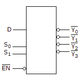
All are HIGH.
All are LOW.
All but  are LOW.
are LOW.All but  are HIGH.
are HIGH.Your Answer: Option
(Not Answered)
Correct Answer: Option
Discuss about this problem : Discuss in Forum
Learn more problems on : Combinational Logic Circuits
7.
Looping on a K-map always results in the elimination of:
Your Answer: Option
(Not Answered)
Correct Answer: Option
Discuss about this problem : Discuss in Forum
Learn more problems on : Combinational Logic Circuits
8.
VHDL was created as a very flexible language and it allows us to define the operation of clocked devices in the code without relying on logic primitives.
Your Answer: Option
(Not Answered)
Correct Answer: Option
Discuss about this problem : Discuss in Forum
Learn more problems on : Flip-Flops
9.
A(n) ________ one-shot starts a pulse in response to a trigger and will restart the internal pulse timer every time a subsequent trigger edge occurs before the pulse is complete.
Your Answer: Option
(Not Answered)
Correct Answer: Option
Discuss about this problem : Discuss in Forum
Learn more problems on : Counters
10.
ROMs retain data when the ________.
Your Answer: Option
(Not Answered)
Correct Answer: Option
Discuss about this problem : Discuss in Forum
Learn more problems on : Memory and Storage
11.
The condition occurring when two or more devices try to write data to a bus simultaneously is called ________.
Your Answer: Option
(Not Answered)
Correct Answer: Option
Discuss about this problem : Discuss in Forum
Learn more problems on : Memory and Storage
12.
Select the statement that best describes Read-Only Memory (ROM).
Your Answer: Option
(Not Answered)
Correct Answer: Option
Discuss about this problem : Discuss in Forum
Learn more problems on : Memory and Storage
13.
Address decoding for dynamic memory chip control may also be used for:
Your Answer: Option
(Not Answered)
Correct Answer: Option
Discuss about this problem : Discuss in Forum
Learn more problems on : Memory and Storage
14.
ROM access time is defined as ________.
Your Answer: Option
(Not Answered)
Correct Answer: Option
Discuss about this problem : Discuss in Forum
Learn more problems on : Memory and Storage
15.
Most PAL devices have a tristate buffer driving the input pins.
Your Answer: Option
(Not Answered)
Correct Answer: Option
Discuss about this problem : Discuss in Forum
Learn more problems on : Programmable Logic Device
16.
The JTAG signals are named TDI, TDO, TMS, and TCK.
Your Answer: Option
(Not Answered)
Correct Answer: Option
Discuss about this problem : Discuss in Forum
Learn more problems on : Programmable Logic Device
17.
An EPM 7128S in a ________ PQFP package has 12 I/O per LAB plus 4 additional input-only pins for a total of 100 pins.
Your Answer: Option
(Not Answered)
Correct Answer: Option
Discuss about this problem : Discuss in Forum
Learn more problems on : Programmable Logic Device
18.
The SUBDESIGN section defines the input and output of the logic circuit block.
Your Answer: Option
(Not Answered)
Correct Answer: Option
Discuss about this problem : Discuss in Forum
Learn more problems on : Describing Logic Circuits
19.
One CASE construct inside another CASE construct is called a do-loop.
Your Answer: Option
(Not Answered)
Correct Answer: Option
Discuss about this problem : Discuss in Forum
Learn more problems on : Digital System Projects Using HDL
20.
A logic circuit that provides a HIGH output if one input or the other input, but not both, is HIGH, is a(n):
Your Answer: Option
(Not Answered)
Correct Answer: Option
Discuss about this problem : Discuss in Forum
Learn more problems on : Ex-OR and Ex-NOR Gates
*** END OF THE TEST ***
Time Left: 00:29:56
Post your test result / feedback here:
Quick links
Quantitative Aptitude
Verbal (English)
Reasoning
Programming
Interview
Placement Papers