Electronics and Communication Engineering - Electronic Devices and Circuits - Discussion
Discussion Forum : Electronic Devices and Circuits - Section 1 (Q.No. 26)
26.
Crossover distortion behaviour is characteristic of
Answer: Option
Explanation:
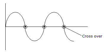
It is a characteristics of class B output stage as the amplifier is biased in cut-off region.
In class B amplifier, two transistor are operated in such a way that one is amplify the half cycle and second is amplify -ve half cycle.
Discussion:
4 comments Page 1 of 1.
Ammu said:
9 years ago
Thanks to all.
(2)
Deepika said:
1 decade ago
Can anyone explain about crossover voltage in detail?
Ravi Grover said:
10 years ago
Crossover is a time delay between output voltage, in Class B amplifier one transistor On for +ve wave and another transistor on for -ve cycle. So the time delay between one transistor on or another transistor on in this delay class B amplifier not working for a short period it is called crossover distortion.
PRAdeep said:
9 years ago
In classB to switch transistor from OFF state to ON state, it requires 0.7v,
If the input is less than 0.7v still transistor is in cut-off even though the positive voltage is applied this causes distortion.
Cross over distortion can be eliminated by using class AB operation.
If the input is less than 0.7v still transistor is in cut-off even though the positive voltage is applied this causes distortion.
Cross over distortion can be eliminated by using class AB operation.
Post your comments here:
Quick links
Quantitative Aptitude
Verbal (English)
Reasoning
Programming
Interview
Placement Papers