Electronics and Communication Engineering - Electronic Devices and Circuits
Exercise : Electronic Devices and Circuits - Section 18
- Electronic Devices and Circuits - Section 14
- Electronic Devices and Circuits - Section 27
- Electronic Devices and Circuits - Section 26
- Electronic Devices and Circuits - Section 25
- Electronic Devices and Circuits - Section 24
- Electronic Devices and Circuits - Section 23
- Electronic Devices and Circuits - Section 22
- Electronic Devices and Circuits - Section 21
- Electronic Devices and Circuits - Section 20
- Electronic Devices and Circuits - Section 19
- Electronic Devices and Circuits - Section 18
- Electronic Devices and Circuits - Section 17
- Electronic Devices and Circuits - Section 16
- Electronic Devices and Circuits - Section 15
- Electronic Devices and Circuits - Section 1
- Electronic Devices and Circuits - Section 13
- Electronic Devices and Circuits - Section 12
- Electronic Devices and Circuits - Section 11
- Electronic Devices and Circuits - Section 10
- Electronic Devices and Circuits - Section 9
- Electronic Devices and Circuits - Section 8
- Electronic Devices and Circuits - Section 7
- Electronic Devices and Circuits - Section 6
- Electronic Devices and Circuits - Section 5
- Electronic Devices and Circuits - Section 4
- Electronic Devices and Circuits - Section 3
- Electronic Devices and Circuits - Section 2
31.
If f(t) = r (t - a), F(s) =
32.
For the network in figure, which of the following expressions gives the value of net inductance between terminals A and B
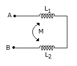
- L1 ± L2
- L1 ± L2 ± M
- L1 ± L2 - 2M
- L1 ± L2 ± 2M
33.
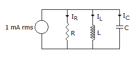
The parallel RLC circuit shown in figure is in resonance. If
34.
An ideal voltage source can not be converted into an equivalent current source.
35.
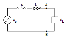
Load ZL for maximum power transfer is
Quick links
Quantitative Aptitude
Verbal (English)
Reasoning
Programming
Interview
Placement Papers