Electronics and Communication Engineering - Electronic Devices and Circuits
Exercise : Electronic Devices and Circuits - Section 17
- Electronic Devices and Circuits - Section 14
- Electronic Devices and Circuits - Section 27
- Electronic Devices and Circuits - Section 26
- Electronic Devices and Circuits - Section 25
- Electronic Devices and Circuits - Section 24
- Electronic Devices and Circuits - Section 23
- Electronic Devices and Circuits - Section 22
- Electronic Devices and Circuits - Section 21
- Electronic Devices and Circuits - Section 20
- Electronic Devices and Circuits - Section 19
- Electronic Devices and Circuits - Section 18
- Electronic Devices and Circuits - Section 17
- Electronic Devices and Circuits - Section 16
- Electronic Devices and Circuits - Section 15
- Electronic Devices and Circuits - Section 1
- Electronic Devices and Circuits - Section 13
- Electronic Devices and Circuits - Section 12
- Electronic Devices and Circuits - Section 11
- Electronic Devices and Circuits - Section 10
- Electronic Devices and Circuits - Section 9
- Electronic Devices and Circuits - Section 8
- Electronic Devices and Circuits - Section 7
- Electronic Devices and Circuits - Section 6
- Electronic Devices and Circuits - Section 5
- Electronic Devices and Circuits - Section 4
- Electronic Devices and Circuits - Section 3
- Electronic Devices and Circuits - Section 2
26.
Laplace transform of tn is


27.
RMS value of a square wave is the same as peak value.
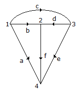
28.
For graph of figure, one set of fundamental cutsets would be
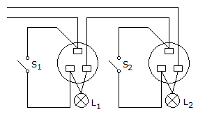
29.
The closing of switch S1 and S2 in figure will light up
30.
Out of Metal-film type and Carbon-film type, the one with better tolerance specification is
Quick links
Quantitative Aptitude
Verbal (English)
Reasoning
Programming
Interview
Placement Papers