Electronics and Communication Engineering - Analog Electronics
Exercise : Analog Electronics - Section 2
- Analog Electronics - Section 11
- Analog Electronics - Section 21
- Analog Electronics - Section 20
- Analog Electronics - Section 19
- Analog Electronics - Section 18
- Analog Electronics - Section 17
- Analog Electronics - Section 16
- Analog Electronics - Section 15
- Analog Electronics - Section 14
- Analog Electronics - Section 13
- Analog Electronics - Section 12
- Analog Electronics - Section 1
- Analog Electronics - Section 10
- Analog Electronics - Section 9
- Analog Electronics - Section 8
- Analog Electronics - Section 7
- Analog Electronics - Section 6
- Analog Electronics - Section 5
- Analog Electronics - Section 4
- Analog Electronics - Section 3
- Analog Electronics - Section 2
16.
In figure, transistor βdc = 100 and LED voltage when it is conducting is 2 V. Then the base current which saturates the transistor is

Answer: Option
Explanation:
 .
.
17.
In figure the dc emitter current of each transistor is about
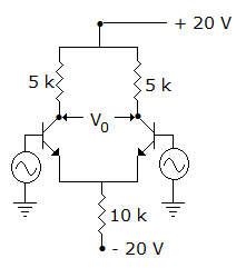
Answer: Option
Explanation:
Total 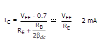 . It divides equally between the two transistors.
18.
The input voltage for starting oscillations in an oscillator is caused by
Answer: Option
Explanation:
The amplifier in the oscillator amplifies the noise voltages. However phase shift around the closed loop is zero at only one frequency. Therefore, only this frequency appears at output.
19.
The current flowing in a certain P-N junction at room temperature is 2 x 10⁻⁷ Amp. When a large reverse biased voltage is applied. Calculate the current flowing when 0.1 volts is applied.
Answer: Option
Explanation:

20.
In following figure find VDSQ by assuming gate current is negligible for the p-channel JFET. (if IDQ = - 6 mA, RS = 0, VDD = -18 V, RD = 2 kΩ, IDSS = - 10 mA, IPO = - 3 V)
Answer: Option
Explanation:
By Appling KVL around drain source loop.
VDSQ = -18 - (-6). 2 x 103 = - 18 + 12 k x 10-3  -6 V.
-6 V.
Quick links
Quantitative Aptitude
Verbal (English)
Reasoning
Programming
Interview
Placement Papers