Electronics and Communication Engineering - Analog Electronics
Exercise : Analog Electronics - Section 2
- Analog Electronics - Section 11
- Analog Electronics - Section 21
- Analog Electronics - Section 20
- Analog Electronics - Section 19
- Analog Electronics - Section 18
- Analog Electronics - Section 17
- Analog Electronics - Section 16
- Analog Electronics - Section 15
- Analog Electronics - Section 14
- Analog Electronics - Section 13
- Analog Electronics - Section 12
- Analog Electronics - Section 1
- Analog Electronics - Section 10
- Analog Electronics - Section 9
- Analog Electronics - Section 8
- Analog Electronics - Section 7
- Analog Electronics - Section 6
- Analog Electronics - Section 5
- Analog Electronics - Section 4
- Analog Electronics - Section 3
- Analog Electronics - Section 2
46.
A non-inverting op-amp summer is shown in figure, the output voltage V0 is
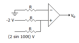

3 sin (100t)
sin (100t)
2 sin (100t)
Answer: Option
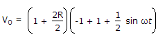
Explanation:
I/p voltage = 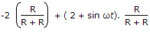

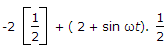
-1 + 1 +  sin ωt sin ωt
 .
.
47.
In following figure find VGG by assuming gate current is negligible for the p-channel JFET. (if IDQ = - 6 mA, RS = 0, VDD = -18 V, RD = 2 kΩ, IDSS = - 10 mA, IPO = - 3 V)
Answer: Option
Explanation:
If Gate current is considered to be negligible then VGG = VGSQ
and 
 .
.
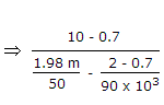
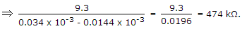
48.
A difference amplifier using op-amp has closed loop gain = 50. If input is 2 V to each of inverting and non-inverting terminals, output is 5 mA. Then CMRR =
Answer: Option
Explanation:
 .
.
49.
The coupling capacitor in amplifier circuits
Answer: Option
Explanation:
Capacitor is open-circuit for dc.
50.
In figure if C is replaced by short circuit then RB will be
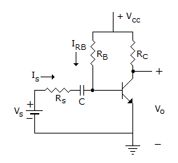
Answer: Option
Explanation:
If C is short circuited then, by using KCL and KVL,
Quick links
Quantitative Aptitude
Verbal (English)
Reasoning
Programming
Interview
Placement Papers