Electronics and Communication Engineering - Electronic Devices and Circuits
Exercise : Electronic Devices and Circuits - Section 5
- Electronic Devices and Circuits - Section 13
- Electronic Devices and Circuits - Section 24
- Electronic Devices and Circuits - Section 23
- Electronic Devices and Circuits - Section 22
- Electronic Devices and Circuits - Section 21
- Electronic Devices and Circuits - Section 20
- Electronic Devices and Circuits - Section 19
- Electronic Devices and Circuits - Section 18
- Electronic Devices and Circuits - Section 17
- Electronic Devices and Circuits - Section 16
- Electronic Devices and Circuits - Section 15
- Electronic Devices and Circuits - Section 14
- Electronic Devices and Circuits - Section 1
- Electronic Devices and Circuits - Section 12
- Electronic Devices and Circuits - Section 11
- Electronic Devices and Circuits - Section 10
- Electronic Devices and Circuits - Section 9
- Electronic Devices and Circuits - Section 8
- Electronic Devices and Circuits - Section 7
- Electronic Devices and Circuits - Section 6
- Electronic Devices and Circuits - Section 5
- Electronic Devices and Circuits - Section 4
- Electronic Devices and Circuits - Section 3
- Electronic Devices and Circuits - Section 2
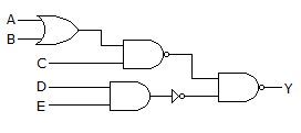
26.
In the given figure, Y =
Answer: Option
Explanation:
 .
.
27.
Assertion (A): The access time of memory is lowest in the case of DRAM
Reason (R): DRAM uses refreshing cycle.
Answer: Option
Explanation:
DRAM has lower speed than SRAM.
28.
In a 3 input NOR gate, the number of states in which output is 1 equals
Answer: Option
Explanation:
Only one input, i.e., A = 0, B = 0 and C = 0 gives 1 as output.
29.
Assertion (A): Even if TTL gates and CMOS gates used in a realization have the same power supply of + 5 V, suitable circuit is needed to interconnect them
Reason (R): VOH, VOL, VIH and VIL of a TTL gave are respectively 2.4, 0.4, 2 and 0.8 V respectively. If supply voltage is + 5 V. VIL and VIH for CMOS gate for the supply voltage of + 5 V are 1.5 V and 3.5 V respectively.
Answer: Option
Explanation:
Interfacing is necessary and interfacing depends on gate parameters like VOH, VOL, IIH, IIL.
30.
The series 54 H/74 H denotes
Answer: Option
Explanation:
It denotes high speed TTL.
Quick links
Quantitative Aptitude
Verbal (English)
Reasoning
Programming
Interview
Placement Papers