Electronics and Communication Engineering - Digital Electronics - Discussion
Discussion Forum : Digital Electronics - Section 1 (Q.No. 13)
13.
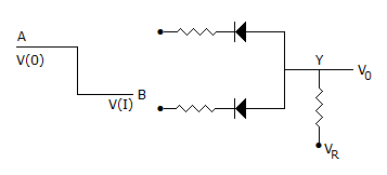
The circuit in the given figure is
Answer: Option
Explanation:
Since V(I) is lower state than V(0) it is a negative logic circuit. Since diodes are in reversed parallel, it is an AND gate.
Note: In Boolean algebra it is recognized that a positive logic OR is a negative logic AND. Similarly a positive logic AND is a negative logic OR.
Discussion:
29 comments Page 3 of 3.
Gyandeep shukla said:
10 years ago
It is positive OR gate.
Denika said:
10 years ago
I am not getting this, Please, anyone can explain this question clearly?
Shruti said:
10 years ago
Yes, it is negative logic AND gate.
Parl said:
10 years ago
It is -ve because 0 volts is shown as a logic high, and 1 volt is shown by logic low.
Irshad said:
10 years ago
@Pava Kumar.
How -ve?
How -ve?
Pava kumar said:
1 decade ago
It is negative logic and gate the above answer is wrong.
Ravi shankar kumar said:
1 decade ago
Since V (1) is lower state than V (0) it is a negative logic circuit. Here diode is not adding at the junction but away from the junction. So it is negative logic AND Gate.
(1)
Pullas said:
1 decade ago
It is negative and gate.
Can said:
1 decade ago
Since V(1) is lower state than V(0) it is a negative logic circuit. Since diodes are in parallel, it is an OR gate.
Post your comments here:
Quick links
Quantitative Aptitude
Verbal (English)
Reasoning
Programming
Interview
Placement Papers