Electronics and Communication Engineering - Analog Electronics
Exercise : Analog Electronics - Section 1
- Analog Electronics - Section 11
- Analog Electronics - Section 21
- Analog Electronics - Section 20
- Analog Electronics - Section 19
- Analog Electronics - Section 18
- Analog Electronics - Section 17
- Analog Electronics - Section 16
- Analog Electronics - Section 15
- Analog Electronics - Section 14
- Analog Electronics - Section 13
- Analog Electronics - Section 12
- Analog Electronics - Section 1
- Analog Electronics - Section 10
- Analog Electronics - Section 9
- Analog Electronics - Section 8
- Analog Electronics - Section 7
- Analog Electronics - Section 6
- Analog Electronics - Section 5
- Analog Electronics - Section 4
- Analog Electronics - Section 3
- Analog Electronics - Section 2
11.
In figure The minimum and maximum load currents are
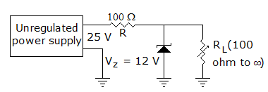
Answer: Option
Explanation:
When RL = ∞, IL = 0,
When RL = 100 Ω,  or 120 mA.
12.
In figure, VEB = 0.6 V, β = 99. Then VC and IC are
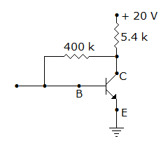
Answer: Option
Explanation:
VC = 20 - 1.98 x 10-3 x 5.4 x 103  9.3 V.
13.
The input impedance of op-amp circuit of figure is
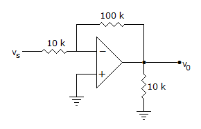
Answer: Option
Explanation:
Due to the presence of virtual ground at input, the resistance in the series path of input of inverting amplifier is input impedance.
14.
In a BJT circuit a pnp transistor is replaced by npn transistor. To analyse the new circuit
Answer: Option
Explanation:
All voltages and currents have reverse polarity.
15.
To protect the diodes in a rectifier and capacitor input filter circuit it is necessary to use
Answer: Option
Explanation:
Resistor reduces surge current.
Quick links
Quantitative Aptitude
Verbal (English)
Reasoning
Programming
Interview
Placement Papers