Electronics and Communication Engineering - Microwave Communication
Assertion (A): PIN diode is used as a fast switch.
Reason (R): PIN diode has very high resistance when reverse biased and very low resistance when forward biased.
A PIN diode has an intrinsic (i) layer between p and n layers. When reverse bias is applied depletion layers are formed at p-i and i-n junctions.
The effective/width of depletion layer increases by the width of i layer. It can be used as a voltage controlled attenuator.
At high frequencies the rectification effect ceases and impedance of diode is effectively that of i layer.
This impedance varies with the applied bias. It is used in high frequency switching circuits, limiters, modulators etc.
1 x 10-6 x 1000 = 0.001.
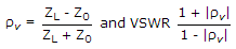
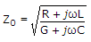
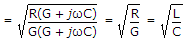
Assertion (A): Impedance measurement at microwave frequencies is done by finding SWR.
Reason (R): SWR and reflection coefficient depend on the characteristic impedance and load impedance.


 or
or 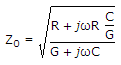
 .
.
A Klystron is a vacuum tube used for generation/amplification of microwaves.
An electron beam is produced by oxide coated indirectly heated cathode and is focussed and accelerated by focussing electrode.
This beam is transmitted through a glass tube. The input cavity where the beam enters the glass tube is called buncher.
As electrons move ahead they see an accelerating field for half cycle and retarding field for the other half cycle.
Therefore, some electrons are accelerated and some are retarded. This process is called velocity modulation.
The velocity modulation causes bunching of electrons. This bunching effect converts velocity modulation into density modulation of beam.
The input is fed at buncher cavity and output is taken at catcher cavity.
In a two cavity klystron only buncher and catcher cavity are used. In multi cavity klystron one or more intermediate cavities are also used.
The features of a multicavity klystron are :
1. Frequency range - 0.25 GHz to 100 GHz
2. Power output - 10 kW to several hundred kW
3. Power gain - 60 dB (nominal value)
4. Efficiency - about 40%.
A multicavity klystron is used in UHF TV transmitters, Radar transmitter and satellite communication.