Electronics and Communication Engineering - Analog Electronics
Exercise : Analog Electronics - Section 17
- Analog Electronics - Section 11
- Analog Electronics - Section 21
- Analog Electronics - Section 20
- Analog Electronics - Section 19
- Analog Electronics - Section 18
- Analog Electronics - Section 17
- Analog Electronics - Section 16
- Analog Electronics - Section 15
- Analog Electronics - Section 14
- Analog Electronics - Section 13
- Analog Electronics - Section 12
- Analog Electronics - Section 1
- Analog Electronics - Section 10
- Analog Electronics - Section 9
- Analog Electronics - Section 8
- Analog Electronics - Section 7
- Analog Electronics - Section 6
- Analog Electronics - Section 5
- Analog Electronics - Section 4
- Analog Electronics - Section 3
- Analog Electronics - Section 2
46.
Harmonic distortion in CB amplifier may be least when the load resistance is
47.
If a common emitter amplifier with an emitter resistance RC has an overall transconductance gain of 1 m A/V, a voltage gain of - 4 and desensitivity of 50, then the value of the emitter resistance R would be
48.
Turn on time of a transistor switch is equal to sum of (where tr is rise time, td is delay time)
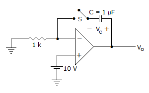
49.
For the circuit shown in the figure, the capacitor C is initially uncharged. At t = 0, the switch S is closed. The voltage Vc across the capacitor at t = 1 millisecond is (In the figure shown above, the op-amp is supplied with ± 15 V and the ground has been shown by the symbol)
50.
In amplifiers, the parasitic oscillation result due to
Quick links
Quantitative Aptitude
Verbal (English)
Reasoning
Programming
Interview
Placement Papers