Electronics and Communication Engineering - Analog Electronics
Exercise : Analog Electronics - Section 5
- Analog Electronics - Section 11
- Analog Electronics - Section 21
- Analog Electronics - Section 20
- Analog Electronics - Section 19
- Analog Electronics - Section 18
- Analog Electronics - Section 17
- Analog Electronics - Section 16
- Analog Electronics - Section 15
- Analog Electronics - Section 14
- Analog Electronics - Section 13
- Analog Electronics - Section 12
- Analog Electronics - Section 1
- Analog Electronics - Section 10
- Analog Electronics - Section 9
- Analog Electronics - Section 8
- Analog Electronics - Section 7
- Analog Electronics - Section 6
- Analog Electronics - Section 5
- Analog Electronics - Section 4
- Analog Electronics - Section 3
- Analog Electronics - Section 2
36.
In figure the voltage drop across diode is 0.7 V. Then the voltage across diode during negative half cycle is
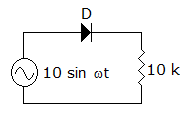
Answer: Option
Explanation:
PIV = 10 V.
37.
In figure vi = 10 mV dc maximum. The maximum possible dc output offset voltage is
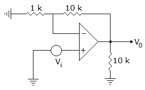
Answer: Option
Explanation:
Maximum dc output offset voltage =  .
.
38.
A transistor with a = 0.9 and ICBO = 10 μA is biased so that IBQ = 90 μA. Then ICQ will be
Answer: Option
Explanation:
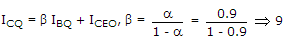
ICEO = (β + 1)ICBO  (9 + 1) 10 μA 100 μA
ICQ = 9 x 90 x 10-6 + 100 x 10-6 = 910 μA.
39.
For the circuit of figure the critical frequency is
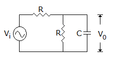


Answer: Option
Explanation:
The two resistances are in parallel.
Critical frequency = 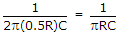 .
.
40.
The current through R1 is(If β = 99, VBE = 0.74 V)
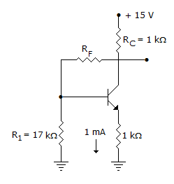
Answer: Option
Explanation:
IE = 1 mA, VBE = 0.7V, β = 99,
IC = aIE, IC = β, IB 1 =

IB = 0.01 mA.
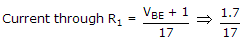
0.1 mA.
Quick links
Quantitative Aptitude
Verbal (English)
Reasoning
Programming
Interview
Placement Papers