Electronics and Communication Engineering - Analog Electronics
Exercise : Analog Electronics - Section 4
- Analog Electronics - Section 11
- Analog Electronics - Section 21
- Analog Electronics - Section 20
- Analog Electronics - Section 19
- Analog Electronics - Section 18
- Analog Electronics - Section 17
- Analog Electronics - Section 16
- Analog Electronics - Section 15
- Analog Electronics - Section 14
- Analog Electronics - Section 13
- Analog Electronics - Section 12
- Analog Electronics - Section 1
- Analog Electronics - Section 10
- Analog Electronics - Section 9
- Analog Electronics - Section 8
- Analog Electronics - Section 7
- Analog Electronics - Section 6
- Analog Electronics - Section 5
- Analog Electronics - Section 4
- Analog Electronics - Section 3
- Analog Electronics - Section 2
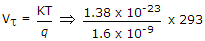
16.
Values of VT at 20°C for an ideal P-N diode
Answer: Option
Explanation:
 .
.
17.
Assertion (A): In an op-amp the voltage gain and band width can be adjusted as per requirement
Reason (R): Large value capacitor can also be fabricated on a chip
Answer: Option
Explanation:
Large value capacitor cannot be fabricated on a chip.
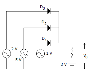
18.
In figure which diode will conduct and what will be the value of V0?
Answer: Option
Explanation:
Since battery connected to anode of D, is of 5 V it is forward biased. D1 and D3 are reverse biased. Output voltage is 5 V.
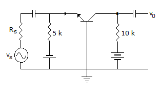
19.
For the amplifier circuit of figure, the h parameters of transistor are hib = 25 Ω, hfb = 0.999, hob = 10-6 Ω. The voltage gain is
Answer: Option
Explanation:
It is a common base circuit 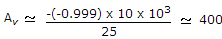 .
.
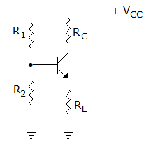
20.
In figure, VCC = + 30 V, R1 = 200 kΩ and R2 = 100 kΩ. If VBE = 0.7 V, the voltage a cross RE =
Answer: Option
Explanation:
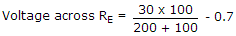 .
.
Quick links
Quantitative Aptitude
Verbal (English)
Reasoning
Programming
Interview
Placement Papers