Electronic Devices - Field-Effect Transistors
Exercise : Field-Effect Transistors - General Questions
- Field-Effect Transistors - General Questions
- Field-Effect Transistors - True or False
21.
In a self-biased JFET circuit, if VD = VDD then ID = ________.
22.
The resistance of a JFET biased in the ohmic region is controlled by
23.
High input resistance for a JFET is due to
24.
For a JFET, the change in drain current for a given change in gate-to-source voltage, with the drain-to-source voltage constant, is
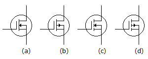
25.
Identify the p-channel E-MOSFET.
Quick links
Quantitative Aptitude
Verbal (English)
Reasoning
Programming
Interview
Placement Papers